

SEMI · Wafer Inspection
Spectra-2000A
Wafer-level 2D optical inspection equipment
High-resolution imaging to accurately identify tiny defects
Automatically identify patterns, etching and appearance abnormalities on the wafer surface through multi-magnification microscopic imaging and AI algorithms
Get product brochure
Please complete the form. Our marketing team will contact you to discuss your requirements.
Core Advantages

High-resolution microscopy imaging
Revealing fine structures and low-contrast anomalies on the wafer surface

Flexible switching of multiple magnifications
Taking into account both large-scale scanning and local high-power review

AI-Powered Defect Recognition
Automatic identification of irregular appearance defects

Autofocus and Calibration
Improve imaging stability and reduce manual intervention
Applications

stain

scratch
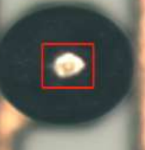
Bump scratch

Collapse
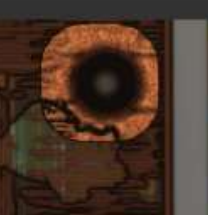
PI hole

Many needle marks
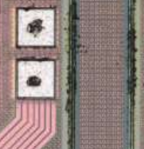
peeling
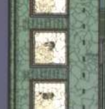
Pad color difference

Pad defect
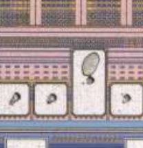
Pad stained