

SEMI · Wafer Inspection
Spectra-3000A
Wafer-level 2D+3D inspection and metrology system
Fusion of 2D and 3D to provide comprehensive insight into wafer defects
Simultaneously obtain wafer surface appearance and spatial topography information to provide accurate and stable quality inspection for wafer manufacturing and advanced packaging
Get product brochure
Please complete the form. Our marketing team will contact you to discuss your requirements.
Product Positioning
Spectra-3000A is oriented towards wafer manufacturing and advanced packaging processes, integrating high-resolution 2D imaging, 3D measurement and AI defect analysis. Achieve comprehensive detection and analysis of wafer surface defects and morphology to meet the strict quality requirements of advanced processes
The equipment can be adapted to Bare Wafers and Wafer on Ring Frames according to the inspection plan.
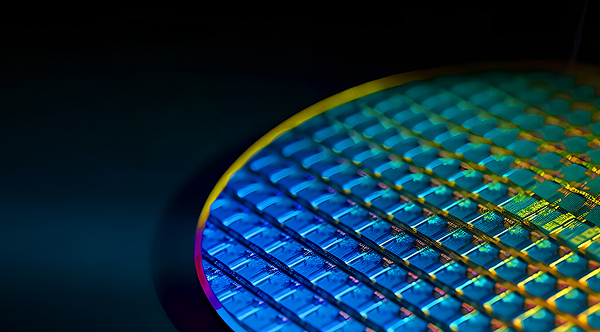
Core Advantages

2D and 3D fusion
Identify anomalies from two dimensions: surface texture and spatial topography.

Multi-Magnification Microscopic Imaging
Taking into account both large-scale inspection and micro-defect observation.

AI-Powered Defect Recognition
Identify complex, low-contrast and irregular defects.

Autofocus and Calibration
Reduce the impact of manual operations on inspection results.
Applications
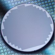
Wafer surface inspection
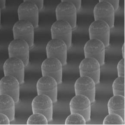
3D morphology of wafer
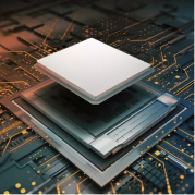
Advanced packaging wafer
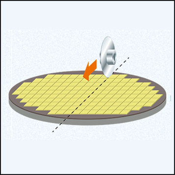
Inspection before and after cutting
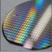
Bare Wafer
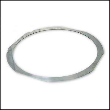
Wafer on Ring Frame
Inspection Capabilities
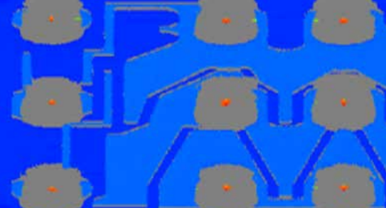
Bumps 3D Imaging
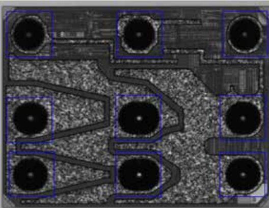
Bumps 2D Imaging
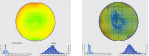
wafer bumps Height Maps